Semiconductor Gallium Nitride Wafer Gan Substrate Template N Type 2 Inch - China
price: check with company for price
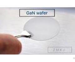
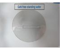
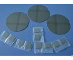
2inch GaN substrates template, GaN wafer for LeD, semiconducting Gallium Nitride Wafer for ld, GaN template, mocvd GaN Wafer, Free-standing GaN Substrates by Customized size, small size GaN wafer for LED, mocvd Gallium Nitride wafer 10x10mm, 5x5mm, 10x5mm GaN wafer # # III-Nitride(GaN, AlN, InN) Gallium Nitride is one kind of wide-gap compound semiconductors.
Gallium Nitride (GaN) substrate is a high-quality single-crystal substrate.
It is made with original HVPE method and wafer processing technology, which has been originally developed for 10+years in China.
The features are high crystalline, good uniformity, and superior surface quality.
GaN substrates are used for many kinds of applications, for white LED and LD(violet, blue and green) Furthermore, development has progressed for power and high frequency electronic device applications.
Forbidden band width (light emitting and absorption) cover the ultraviolet, visible light and infrared.
GaN can be used in many areas such as LED display, High-energy Detection and Imaging, # # Laser Projection Display, Power Device, etc.
# Date storage # Energy-efficient lighting # Full color fla display # Laser Projecttions # High- Efficiency Electronic devices # High- Frequency Microwave Devices # High-energy Detection and imagine # New energy solor hydrogen technology # Environment Detection and biological medicine # Light source terahertz band Specifications: - - - - | Free-standing GaN Substrates (Customized size) | Item | GaN-FS-10 | GaN-FS-15 | Dimensions | 10.0mm10.5mm | 14.0mm15.0mm | Marco Defect Density | A Level | 0 cm-2 | B Level | 2 cm-2 | Thickness | Rank 300 | 300 25 m | Rank 350 | 350 25 m | Rank 400 | 400 25 m | Orientation | C-axis(0001) 0.5 | TTV ( Total Thickness Variation) | 15 m | BOW | 20 m | Conduction Type | N-type | Semi-Insulating | Resistivity(300K) | < 0.5 cm | >106 cm | Dislocation Density | Less than 5x106 cm-2 | Useable Surface Area | > 90% | Polishing | Front Surface: Ra < 0.2nm.
Epi-ready polished | Back Surface: Fine ground | Package | Packaged in a class 100 clean room environment, in single wafer containers, under a nitrogen atmosphere.
| - - - - - - - - Item | GaN-FS-N-1.5 | Dimensions | 25.4mm 0.5mm | 38.1mm 0.5mm | 40.0mm 0.5mm | 45.0mm 0.5mm | Marco Defect Density | A Level | 2 cm-2 | B Level | > 2 cm-2 | Thickness | 300 25 m | Orientation | C-axis(0001) 0.5 | Orientation Flat | (1-100) 0.5 | (1-100) 0.5 | (1-100) 0.5 | (1-100) 0.5 | 8 1mm | 12 1mm | 14 1mm | 14 1mm | Secondary Orientation Flat | (11-20) 3 | (11-20) 3 | (11-20) 3 | (11-20) 3 | 4 1mm | 6 1mm | 7 1mm | 7 1mm | TTV(Total Thickness Variation) | 15 m | BOW | 20 m | Conduction Type | N-type | Semi-Insulating | Resistivity(300K) | < 0.5 cm | >106 cm | Dislocation Density | Less than 5x106 cm-2 | Useable Surface Area | > 90% | Polishing | Front Surface: Ra < 0.2nm.
Epi-ready polished | Back Surface: Fine ground | Package | Packaged in a class 100 clean room environment, in single wafer containers, under a nitrogen atmosphere.
| - - - - Our FactroyEnterprise Vision we will provide high quality GaN substrate and application technology for the industry with our factory.
High quality GaNmaterial is the restraining factor for the III-nitrides application, e.g. long life and high stability LDs, high power and high reliability micro-wave devices, High brightness and high efficiency, energy-saving LED.
-FAQ Q: What you can supply logistics and cost? (1) We accept DHL, Fedex, TNT, UPS, EMS, SF and etc.
(2) If you have your own express number, it's great.
If not, we could assist you to deliver.
Freight=USD25.0(the first weight) + USD12.0/kg Q: What's the delivery time? (1) For the standard products such as 2inch 0.33mm wafer.
For inventory: the delivery is 5 workdays after order.
For customized products: the delivery is 2 or 4workweeks after order.
Q: How to pay? 100T/T, Paypal, West Union, , Secure payment and Trade Assurance.
Q: What's the MOQ? (1) For inventory, the MOQ is 5pcs.
(2) For customized products, the MOQ is 5pcs-10pcs.
It depends on quantity and technics.
Q: Do you have inspection report for material? We can supply ROHS report and reach reports for our products.
Company Contact:
- Posted By: SHANGHAI FAMOUS TRADE CO.,LTD
- Phone: 86-512-36829962
- Address: Rm1-607,No.231,Lvdi Road, Huaqiao town, Kunshan city,jiangsu Province, Kunshan , Jiangsu , China
- Email:

- Website: https://www.galliumnitridewafer.com
Published date: March 19, 2018
- Business Description: As a result of our high quality products and outstanding customer service, we have gained a global sales network reaching If you are interested in any of our products or would like to discuss a custom order, please feel free to contact us.
Related listings
-
 Wurtzite Crystal Structure Led Wafer Gan Gallium Nitride Substrates TemplateMetal treatment machinery - SHANGHAI FAMOUS TRADE CO.,LTD - China - March 19, 2018 - check with company for price
2inch GaN substrates template, GaN wafer for LeD, semiconducting Gallium Nitride Wafer for ld, GaN template, mocvd GaN Wafer, GaN Specifications/Special Features: # # Gallium nitride (GaN) is a very hard madematerial that has a wurtzite crystal struc...
-
 Laser Projection Display Gallium Nitride Wafer 330um Thickness White ColorMetal treatment machinery - SHANGHAI FAMOUS TRADE CO.,LTD - China - March 19, 2018 - check with company for price
2inch free-standing GaN substrates, GaN wafer for LD, semiconducting Gallium Nitride Wafer for led, GaN template, 10x10mm GaN substrates, native GaN wafer, # # III-Nitride(GaN, AlN, InN) Forbidden band width (light emitting and absorption) cover the ...
-
 N Type Gallium Arsenide Wafer Gaas Single Crystal Substrates 2 6 InchMetal treatment machinery - SHANGHAI FAMOUS TRADE CO.,LTD - China - March 19, 2018 - check with company for price
3inch GaAs substrates, GaAs wafer for led, Gallium Arsenide crystal Wafers, Si/Zn Dopant GaAs wafer (A compound of the elements gallium and arsenic. It is a III-V direct bandgap semiconductor with a zinc blende crystal structure) GaAs) Gallium Arseni...
Safe Trade Tips
- Ask for business references and check them
- Use a payment method that offers better protection for all such as Letters of credit and verified professional escrow services. Avoid payments in advance such as money transfers
- Verify their business via their local Chamber of Commerce
- Search the internet using their website address, their business name, their phone and fax numbers, and their email addresses to see if you can find any feedback about them.
- Get to know more about scams and fraud to avoid: Internet Crime Complaint Center - Consumer Financial Protection Bureau
- This site is never involved in any transaction, and does not handle payments, shipping, guarantee transactions, provide escrow services, or offer "buyer protection" or "seller certification"