European and Premium listings
-
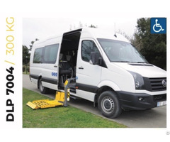 Single Arm Wheelchair Lift 7004Vehicle bodies and trailers - D.L.P LIFT - Turkey (Tekkeköy ) - 1350.00
Single arm wheelchair lift can be used for buses and mini-buses. It is possible to mounting lift from the side door or back door of the vehicle. Lifting lowering and roll stop works automatically. Sliding platform enters nested. It is swivel table an...
-
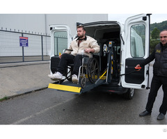 Double Arm Wheelchair Lift 7005Vehicle bodies and trailers - D.L.P LIFT - Turkey (Tekkeköy ) - 1700.00
Double arm wheelchair lift can be used for buses and mini-buses. It is mounting from the back door of the vehicle. Lifting-lowering, opening-closing and roll stop works automatically. Platform opening-closing works automatically. With manuel discharg...
gallium arsenide wafer gaas crystal substrates Photos Catalog - ECeurope Market
-
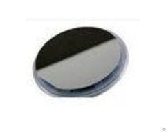
 N Type Gallium Arsenide Wafer Gaas Single Crystal Substrates 2 6 InchMetal treatment machinery - SHANGHAI FAMOUS TRADE CO.,LTD - China - March 19, 2018 - check with company for price
3inch GaAs substrates, GaAs wafer for led, Gallium Arsenide crystal Wafers, Si/Zn Dopant GaAs wafer (A compound of the elements gallium and arsenic. It is a III-V direct bandgap semiconductor with a zinc blende crystal structure) GaAs) Gallium Arseni...
-
 Wurtzite Crystal Structure Led Wafer Gan Gallium Nitride Substrates TemplateMetal treatment machinery - SHANGHAI FAMOUS TRADE CO.,LTD - China - March 19, 2018 - check with company for price
2inch GaN substrates template, GaN wafer for LeD, semiconducting Gallium Nitride Wafer for ld, GaN template, mocvd GaN Wafer, GaN Specifications/Special Features: # # Gallium nitride (GaN) is a very hard madematerial that has a wurtzite crystal struc...
-
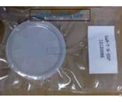
 Dia 50 8mm 2 Inch Gallium Arsenide Wafer For Semiconductor SubstrateMetal treatment machinery - SHANGHAI FAMOUS TRADE CO.,LTD - China - March 19, 2018 - check with company for price
2inch GaAs substrates, GaAs wafer for led, Gallium Arsenide crystal Wafers, Si/Zn Dopant GaAs wafer(A compound of the elements gallium and arsenic. It is a III-V direct bandgap semiconductor with a zinc blende crystal structure) Application: 1. Mainl...
-
 Hvpe Gallium Nitride Wafer Customized Size Free Standing Gan Single Crystal MaterialMetal treatment machinery - SHANGHAI FAMOUS TRADE CO.,LTD - China - March 19, 2018 - check with company for price
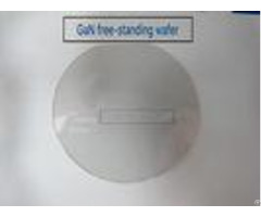
2inch GaN substrates template, GaN wafer for LeD, semiconducting Gallium Nitride Wafer for ld, GaN template, mocvd GaN Wafer, Free-standing GaN Substrates by Customized size, small size GaN wafer for LED, mocvd Gallium Nitride wafer 10x10mm, 5x5mm, 1...
-
 Semiconductor Gallium Nitride Wafer Gan Substrate Template N Type 2 InchMetal treatment machinery - SHANGHAI FAMOUS TRADE CO.,LTD - China - March 19, 2018 - check with company for price
2inch GaN substrates template, GaN wafer for LeD, semiconducting Gallium Nitride Wafer for ld, GaN template, mocvd GaN Wafer, Free-standing GaN Substrates by Customized size, small size GaN wafer for LED, mocvd Gallium Nitride wafer 10x10mm, 5x5mm, 1...
-
 Undoped Semi Insulating Gallium Nitride Wafer Hvpe And Template TypeMetal treatment machinery - SHANGHAI FAMOUS TRADE CO.,LTD - China - March 19, 2018 - check with company for price
2inch HVPE method Gallium Nitride GaN wafer, free standing GaN substrates for LD, 10x10mm size GaN chips, HVPE GaN wafer About GaN FeatureIntroduce - - - - The growing demand for high-speed, high-temperature and high power-handling capabilities has m...
-
 Laser Projection Display Gallium Nitride Wafer 330um Thickness White ColorMetal treatment machinery - SHANGHAI FAMOUS TRADE CO.,LTD - China - March 19, 2018 - check with company for price
2inch free-standing GaN substrates, GaN wafer for LD, semiconducting Gallium Nitride Wafer for led, GaN template, 10x10mm GaN substrates, native GaN wafer, # # III-Nitride(GaN, AlN, InN) Forbidden band width (light emitting and absorption) cover the ...
-
 Tgg Terbium Gallium Garnet Laser CrystalIndustrial optics - Photonchina Co.,Ltd - China - May 30, 2022 - 38.00 Dollar US$
Terbium Gallium Garnet(TGG), as a magneto-optical crystal, is an optimum material for Faraday devices (Rotator and Isolator) in the range from 400nm-1100nm, excluding 470-500nm.The Faraday rotator consists of a TGG rod contained inside a special desi...
-
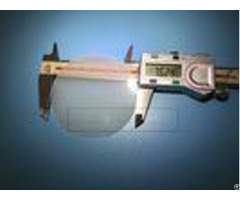
 Al2o3 Single Crystal Sapphire Glass Lens Applied Semiconductor SubstratesMetal treatment machinery - SHANGHAI FAMOUS TRADE CO.,LTD - China - March 18, 2018 - check with company for price
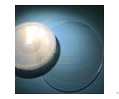
sapphire optical lens, Al2O3 single crystal glass window, double side polished sapphire plates by random orientation, A-plane, M-plane, R-plane sapphire glass plates Why choose the sapphire? Sapphire is a precious gemstone, a variety of the mineral c...
-
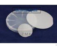
 C Axis 6 Inch Sapphire Wafer Al2o3 Crystal Optical Lens For Led Epi ReadyMetal treatment machinery - SHANGHAI FAMOUS TRADE CO.,LTD - China - March 19, 2018 - check with company for price
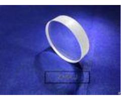
6inch C-axis double side polished sapphire wafer for led epi-ready, sapphire substrates, Al2O3 crystal optical lens Our sapphire material is made by Kyropoulos & Bagdasarov Methods for high purity requirements such as:LED Semiconductors Precision...
-
 C Axis Sapphire Wafer Single Side Polished 3 Inch Al2o3 Crystal Optical LensMetal treatment machinery - SHANGHAI FAMOUS TRADE CO.,LTD - China - March 19, 2018 - check with company for price
3inch C-axis double side polished sapphire wafer for led epi-ready, 3inch sapphire substrates, M-axis, R-axis, A-axis Al2O3 crystal optical lens 1. Sapphire introduction description # # OEM sapphire wafer by china manufacturer, optical sapphire cryst...
-
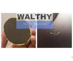 Cvd Diamond Substrates And MetallizationMachining and processing services - Walthy Precision Co., Ltd. - China - October 20, 2021 - 100.00 Dollar US$
CVD Diamond has been recognized an ideal material for various applications because of its outstanding properties which includes extreme hardness and strength, high thermal conductivity, low thermal expansion, excellent dielectric properties, resistan...
-
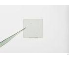
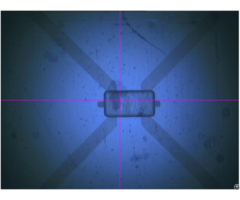 Customized Patterned Ito SubstratesElectronic hardware and component parts and accessories - Walthy Precision Co., Ltd. - China - June 9, 2019 - 1.00 Dollar US$
Patterning ITO substrates Customized Capabilities: ITO coated on glass or PET film(one side or both sides are all available) Coating thickness: 10nm-10um Subsrtate: Glass, PET, quartz, ceramics etc. Pattern min line width: 2-10um (R&D), recommend...
-
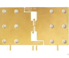
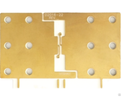
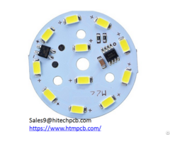 Aluminum Nitride And Alumina Ceramic Substrates PcbPrinted circuits and integrated circuits and microassemblies - Hitech Circuits Co., Limited - China - June 24, 2020 - 10.00 Dollar US$
Aluminum Nitride & Alumina Ceramic Substrates Printed Circuit Board Material: Ceramic ALN Unit size/mm: 10.3*20.3 Finished Thickness : 1.03mm Outer Copper: H oz Surface treatment: Hard gold Gold thickness: 120u" Profiling: Laser cutting Aluminum ...
-
 Slitong Pcb Custom Design Service For Ceramic Metallized SubstratesPrinted circuits and integrated circuits and microassemblies - Folysky Technology(Wuhan)Co.,Ltd - China - August 7, 2019 - 1.00 Dollar US$
Slitong ceramic substrate suppliers have more high-end PCB materials that can be supplied in a timely manner, and ceramic circuit board manufacturers have more advantages. Substrate material thickness:0.635mm Condu cting layer:Cu, Ni, Au Thickness of...
-
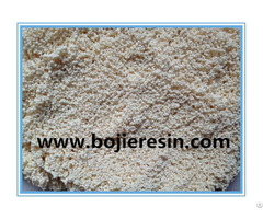
 Special Resin For Gallium ExtractionSolvents - Suzhou Bojie Resin Technology Co.,Ltd - China - December 23, 2020 - 10.00 Dollar US$
Gallium is a rare blue-white trivalent metal element that is soft and hard and brittle at low temperatures. Usually obtained as a by-product from the extraction of aluminum from bauxite or the extraction of zinc from zinc ore - the element symbol Ga....
-
 Slitong Custom Design Service For Ceramic Circuit Board Metallized SubstratesElectrical equipment and components - Folysky Technology(Wuhan)Co.,Ltd - China - February 16, 2020 - 1.20 Dollar US$
Substrate material thickness:0.635mm Condu cting layer:Cu, Ni, Au Thickness of metal layer:300μm Surface preparation:immersion gold Ceramic pcb vendor:Slitong ceramic PCB Metal single-sided / double sided:single sided Copper plated through hole:no So...
-
 Sgs Rohs Uv Led Ink 385 395nm Wavelength For Plastics And Tinplate SubstratesLivestock services - Shenzhen Meilianxing Technology CO., LTD. - China - January 10, 2018 - contact company for price
UV LED Offset Inks for Papers, Plastics and Tinplate substrates We Meilianxing is already 17 years in UV ink, and we develop UV LED ink since the year 2014, after so many experiment & testing on different brand LED UV curing system and mutiple su...
-
 Gallium Extraction From Mother Liquor By Bayer ProcessAdditives - suzhou bojie resin technology co.,ltd - China - February 4, 2024 - 10.00 Dollar US$
Because metal gallium is widely used and expensive, it is of great significance to extract and recycle it. Currently, 90% of primary gallium is mainly recovered from Bayer sodium aluminate solution of bauxite ore, and the remaining 10% is mainly deri...
-
 Chelating Resin For Extraction Gallium From Bayer Mother LiquorWater and wastewater treatment supply and disposal - suzhou bojie resin technology co.,ltd - China - December 17, 2020 - 10.00 Dollar US$
Gallium is an alloy semiconductor material with excellent properties and its natural resources are scarce. About 90% of the world's gallium is obtained from the seed liquid of Bayer process for the production of Al2O3. The ion exchange method is the ...